
Specify the deposit, not just “gold”
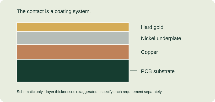
Hard gold identifies an alloyed gold deposit used where contact wear matters. On a PCB, it is commonly applied electrolytically to selected contact areas over a nickel underplate. The required deposit chemistry, thickness, hardness where applicable and inspection method belong in the manufacturing agreement. A gold-colored surface cannot demonstrate any of those properties.
Separate contact and assembly requirements
Wear contacts and component lands have different jobs. Mark the hard gold region explicitly in the fabrication data, then specify the finish for solderable pads independently. Avoid extending an edge-contact requirement to every exposed copper feature by accident. Review the boundary between finishes, local masking and component keepouts with the fabricator before release.
| Callout | Reason it matters |
|---|---|
| Gold deposit type | “Hard gold” and “immersion gold” describe different processes. |
| Minimum local thickness | A nominal average does not establish the thinnest acceptable location. |
| Nickel underplate | The complete coating system, not only the top layer, affects the contact. |
| Measurement plan | Agree locations, methods, sampling and records. |
| Selective region | Communicate both sides and all intended wear areas. |
Allow for electrical access during plating
Electrolytic deposition needs an electrical path to the regions being plated. Temporary connections and panel features can be involved, and their eventual removal must be reviewed. Do not assume a panel layout or plating bus can be added without affecting signal routing or edge clearances. Ask how the approved process handles isolated contacts and the final outline.
Balance wear, environment and cost
There is no universal thickness that guarantees a fixed mating life. Use connector qualification and actual operating conditions to choose the finish system. The gold material model can illustrate how area and thickness affect ideal gold mass, but it excludes processing, panel utilization, losses, testing and supplier pricing.
Questions to resolve in your inquiry
State whether the contact will be mated once during assembly or repeatedly in service, identify the mating finish, and describe contamination or vibration exposure. If you have a qualified legacy design, provide its approved drawing and change constraints rather than inferring the specification from a sample’s appearance.
Have a drawing to review? Send your gold finger PCB requirements with the connector part number, quantities and any open questions. Files are optional.