
The purpose of the entry geometry
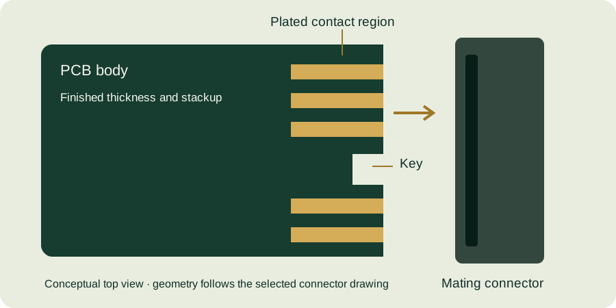
A shaped board edge helps the card enter the intended connector interface. The correct shape depends on the connector’s drawing and the finished board geometry. Do not assume every gold finger PCB needs the same bevel or that a familiar angle is automatically suitable for a new connector.
An angle needs a reference
An angle measured from the board surface differs from one measured from the board edge. Show the cross-section and the angle datum explicitly. State whether the bevel applies on one or both faces, and identify the final profile. A written angle without a sketch can be interpreted in conflicting ways.
| Dimension or note | Question it resolves |
|---|---|
| Finished board thickness | What thickness enters the connector before the bevel? |
| Angle and datum | From which surface is the angle measured? |
| Residual tip thickness | How much material remains at the leading edge? |
| Bevel extent | How far does the cut extend back from the final edge? |
| Copper clearance | What remains clear under the allowed tolerances? |
| Affected edges | Which specific portions of the outline receive the operation? |
Review the tolerance extremes
The cutting geometry, board thickness and routed edge position all contribute to the final shape. Check whether the allowable combination exposes copper, removes part of the usable contact area or conflicts with the connector entry. Include inner-layer copper in the review; a visible outer-layer clearance alone does not prove the whole cross-section is safe.
Keep the contact area and bevel distinct
The mating contact should travel over the intended plated surface according to the connector design. Communicate the relationship between the contact endpoint, wipe area and shaped edge. Do not assume the bevel itself is a functional plated contact surface unless the actual design and manufacturing process explicitly require and support that construction.
A drawing review that prevents rework
Provide a dimensioned cross-section, top view and connector reference together. Ask the fabricator to flag any conflict between machining, plating and final inspection before manufacture. The design readiness checklist is a useful place to record open geometry questions rather than silently filling them with a generic standard.
Have a drawing to review? Send your gold finger PCB requirements with the connector part number, quantities and any open questions. Files are optional.