
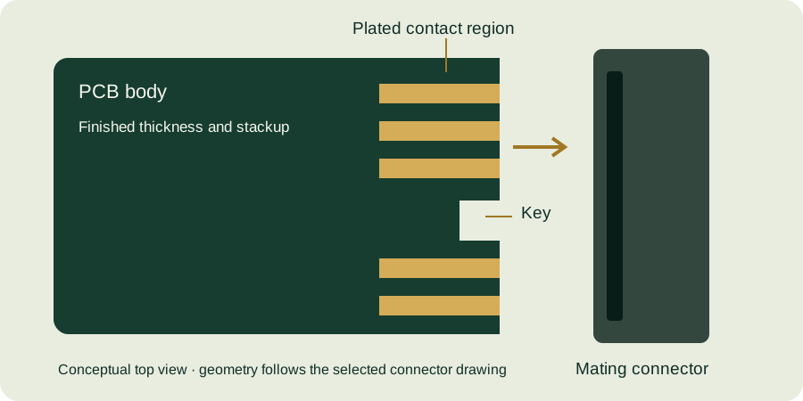
1. Begin with the mating connector
Obtain the exact component drawing and confirm its revision. Record contact pitch, pad dimensions, card thickness range, insertion depth, keying and recommended entry shape. Avoid drawing a generic row of fingers and selecting the connector afterward. For a replacement design, identify which legacy dimensions are actually controlled and which were inherited without justification.
2. Establish one mechanical datum
Use a clear datum for the contact pattern, final routed edge and keys. State dimensional tolerances where fit depends on them. Include finished thickness at the mating zone and distinguish it from a nominal laminate thickness. If the assembly has a bracket or enclosure guide, show how those references relate to the connector.
3. Define the entire contact zone
Show pad width, pitch, usable contact length and side orientation. Identify the region swept by the mating contact and keep incompatible features outside it. Do not place solder mask, legend, test damage or assembly residue in the intended contact path. Different contact lengths require a system-level sequencing rationale; verify pin mapping and insertion direction before implementing them.
4. Review the bevel as a cross-section
Specify the angle reference, residual tip thickness, bevel depth or other controlling dimensions, and whether both sides are treated. Check the worst-case relationship to copper and inner layers. The beveling guide shows the questions a single angle callout leaves unresolved.
5. Specify a complete finish system
State the deposit type, minimum gold thickness, nickel requirement, selective region and measurement plan. Identify the finish elsewhere on the PCB. A note such as “gold fingers” does not establish those details. Use the thickness converter and guide to keep microinches and micrometers consistent.
6. Check routing and plating access together
Review the electrical path needed to plate the contacts and how any temporary connections are removed. For high-speed signals, assess the connector launch, reference planes and remaining features in the final design. Share a proposed panel or routing restriction when it is part of the product requirement rather than leaving it implicit.
7. Define acceptance before manufacture
Agree which dimensions and coating properties will be measured, where they will be checked and which records are needed. Include an inspection plan appropriate to the application. Appearance, electrical continuity and finish thickness answer different questions; none alone proves the full connector system is qualified.
8. Release one consistent package
Check that the drawing, Gerber or other agreed manufacturing data, drill files, netlist, stackup and quote request all use the same revision. Remove obsolete alternatives from the release package or label them clearly. Retain the approved package and any accepted deviations so production can repeat the intended design.
Have a drawing to review? Send your gold finger PCB requirements with the connector part number, quantities and any open questions. Files are optional.