
The board edge is part of the connector
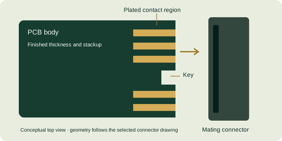
A gold finger PCB uses conductive contacts along a board edge to make a removable electrical connection. The contacts are not simply decorative gold pads. They must enter the connector correctly, stay within its contact travel, and maintain the intended electrical interface over the product’s use. Start with the mating connector drawing and the system requirements, then specify the PCB to match.
Build the specification from the interface outward
Identify the exact connector manufacturer, part number and drawing revision. Record its permitted card thickness and tolerance, insertion depth, contact pitch, key positions and recommended entry geometry. Separate dimensions controlled by the connector from dimensions controlled by the enclosure. A nominal board thickness alone does not establish a fit: the final thickness tolerance and local build-up at the mating area matter.
| Design input | What to put in the inquiry |
|---|---|
| Application | Removable module, test fixture, backplane card or another defined use. |
| Mechanical interface | Connector drawing, finished thickness and tolerance, contact dimensions and edge datum. |
| Surface finish | Deposit type, minimum gold and nickel thickness, selective areas and measurement locations. |
| Use conditions | Expected insertion/removal, vibration, temperature, humidity and contamination. |
| Delivery package | Fabrication drawing, copper data, drills, stackup, quantity and revision. |
Choose the contact finish deliberately
Repeated mating often calls for electrolytic hard gold on the wear surface. It is different from a solderability finish such as ENIG. The rest of the board may need a separate finish selected for assembly. Specify both areas clearly and review the transition between them. Our finish comparison explains the distinction; the thickness guide helps avoid ambiguous units.
Keep the mechanical and electrical reviews connected
The edge profile, plating access and routing affect each other. Check copper clearances after the bevel is cut, any temporary plating connections, connector pin numbering and ground-return paths. If contacts have different lengths for sequencing, their order must come from the complete mating system design. A shorter pad by itself is not a validated hot-plug feature.
What happens before a production commitment
Use the inquiry to establish which requirements are fixed and which require review. Ask for feedback on any unresolved connector fit, finish callout, material or inspection requirement. Confirm approved drawings and acceptance criteria before ordering; this page does not establish a guaranteed fabrication tolerance, capacity or delivery date.
Have a drawing to review? Send your gold finger PCB requirements with the connector part number, quantities and any open questions. Files are optional.