
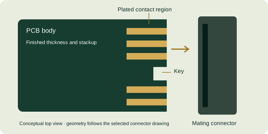
One interface, several interacting layers
A multilayer card-edge design must satisfy the connector’s mechanical envelope while routing signals and power through a layered structure. The number of layers is only one input. Finished thickness, material properties, copper distribution and the transition into the contact region need to be reviewed together. Start with a proposed stackup that can be checked against the connector drawing.
Make the finished thickness measurable
Specify final board thickness and tolerance at the location relevant to mating. Include any local thickness requirement rather than assuming the overall stackup drawing covers the contact area. Identify the measurement basis, such as whether a value refers to laminate, copper build-up or finished surfaces. Ask the fabricator to confirm the achievable stackup before locking connector and enclosure dimensions.
Treat the connector launch as part of the channel
For high-speed interfaces, use the connector vendor’s recommended footprint and modeling guidance. The edge contacts, pad geometry, vias and changes in reference plane can all influence the transition. Controlled impedance on a straight trace does not by itself validate the connector launch. Keep the intended return path visible in layout and review any reference-plane changes or nearby cutouts.
- Provide target impedances, routing layers and the relevant reference planes.
- Identify differential pairs and any length or skew constraints from the system budget.
- Separate mechanical keepouts, copper keepouts and component keepouts.
- Check whether plating connections leave features requiring signal-integrity review.
- Include drill information, layer order and the drawing revision in one consistent package.
Prototype the risks you cannot settle on paper
A prototype should answer defined questions: fit at thickness extremes, contact wipe location, assembled clearances or channel behavior. Keep the tested finish, stackup and connector revision traceable so a later production change does not quietly invalidate the result. Decide which measurements will be repeated when materials or suppliers change.
Related engineering resources
Use the gold finger design guide for the interface review, HDI guidance when breakout density becomes a constraint, and inspection guide to define acceptance evidence.
Have a drawing to review? Send your gold finger PCB requirements with the connector part number, quantities and any open questions. Files are optional.