
Use density where it solves a defined problem
HDI construction can help route a dense assembly, but microvias do not remove the need for a clear card-edge interface. Define the connector geometry and stackup first, then identify which breakout regions genuinely require finer interconnects. Extra build-up cycles, dense routing and complex via structures introduce manufacturing and verification decisions that should be reviewed early.
Document the via structure explicitly
List the via spans and intended construction in the stackup. Distinguish through holes, blind vias, buried vias and microvias instead of relying on a generic “HDI” label. State whether filling, capping or via-in-pad processing is needed in any region. The chosen fabricator must assess the actual material set and process sequence; this page does not imply every via architecture is supported.
Keep the gold finger region manufacturable
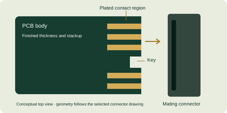
Plating access, edge milling and beveling need space and a consistent datum. Review the contact area separately from dense component escape routing. Avoid hiding a mechanical clearance requirement in a copper layer note. The contact geometry should remain tied to the connector drawing even when other parts of the layout are optimized aggressively.
Validate the complete high-speed path
Use connector models appropriate to the part and configuration. Include launch discontinuities, vias, routing and reference-plane transitions in the system analysis when the application requires it. A board’s layer count or a finish label cannot establish a supported data rate. Confirm the analysis assumptions with the actual stackup, trace geometry and connector model revision.
| Before layout freeze | Evidence to review |
|---|---|
| Connector launch | Footprint, pin assignment, model and mechanical drawing revisions. |
| Stackup | Materials, thickness, copper and impedance targets. |
| Via architecture | Layer spans, fill/cap requirements and fabrication review. |
| Edge contacts | Finish area, plating approach, profile and bevel clearances. |
| Validation | Defined electrical and mechanical tests for the intended application. |
Choose the next design step
If routing fits a conventional stackup, compare the simpler multilayer approach before adding complexity. For unresolved geometry, attach the current design and describe the constraint in a technical inquiry.
Have a drawing to review? Send your gold finger PCB requirements with the connector part number, quantities and any open questions. Files are optional.