
A process overview, not a universal routing sheet
The exact order of fabrication operations depends on the board structure, finish combination and approved process. The useful starting point is to understand what each operation must achieve and which design information it needs. A generic process diagram cannot replace the fabricator’s reviewed production plan.
1. Review files and construction
Confirm the board revision, stackup, contact pattern, connector reference and finish map. Resolve inconsistent thickness units or competing dimensions before work starts. Review materials, drilling, copper requirements and any high-speed or reliability constraints as one package.
2. Plan the panel and plating connections
Electrolytic processing requires suitable electrical access to the plated regions. The panel and temporary conductive features must support that process and permit the intended final outline. Review how such features are removed and whether remnants affect the final electrical design.
3. Fabricate and prepare the surfaces
The board structure is built and the relevant surfaces prepared under the approved manufacturing process. Surface condition matters to the coating system. The specific preparation and masking steps depend on the materials and finish sequence; do not substitute a generic cleaning recipe into a qualified process.
4. Apply the specified coating system
The nickel and gold requirements should be explicit, including selective areas and acceptance limits. Control and verify the process through the agreed quality plan. Record the measurement locations and sampling required by the order rather than relying only on a visual impression of the finished contacts.
5. Complete the edge geometry
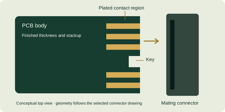
Routing, keying and beveling must leave the final mating geometry shown on the drawing. Their sequence relative to finishing depends on the actual process. Confirm the final edge, copper clearance and contact region after all relevant operations, including removal of temporary features.
6. Inspect, test and protect
Review electrical test results, critical dimensions and finish evidence according to the agreed acceptance plan. Handle and package contacts to avoid contamination and mechanical damage. Any deviation should be recorded and resolved through the agreed disposition process before shipment.
What the designer can do to reduce ambiguity
Provide a dimensioned bevel cross-section, a clear finish thickness requirement and a traceable release package. If a process choice is important to function, include it in the requirement rather than assuming every supplier follows the same sequence.
Have a drawing to review? Send your gold finger PCB requirements with the connector part number, quantities and any open questions. Files are optional.