
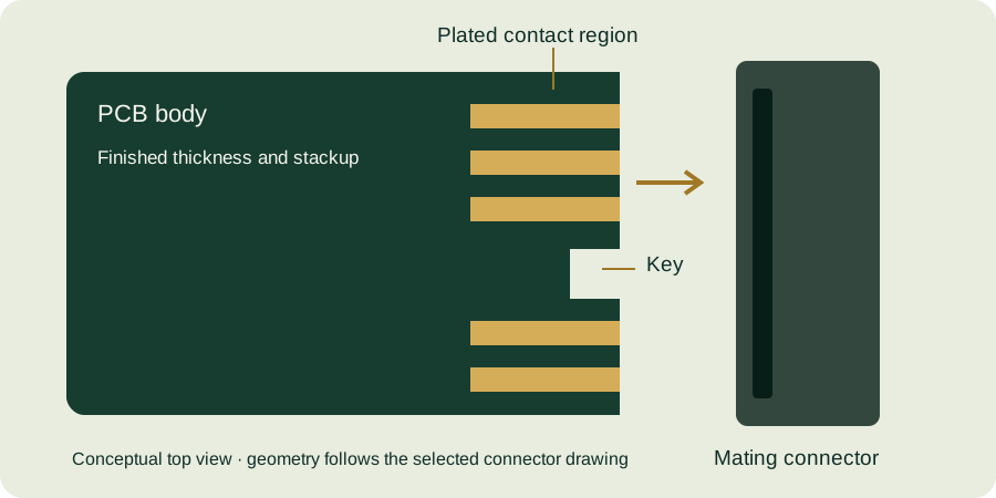
Gold fingers turn the edge of a printed circuit board into a removable electrical interface. Instead of soldering a cable to the board, a card-edge connector presses its spring contacts against plated copper pads. The board can then be installed, tested or replaced without unsoldering the interface. A successful design treats the board and connector as one system: contact dimensions, board thickness, finish and insertion geometry all need to agree.
What the fingers actually connect
Each finger provides a conductive contact surface connected to a circuit on the PCB. Depending on the design, those circuits can carry power, ground or signals. The gold-colored surface is only one part of the path. Copper connects the pad to the rest of the board, and the mating connector supplies the spring contact that touches the pad. Electrical continuity therefore depends on both parts being correctly aligned and maintained.
The number of visible fingers does not by itself establish the pin assignment. A double-sided card can have different circuits on opposite faces, and a key notch can interrupt the sequence. Use a connector pin map and an unambiguous view convention in the design package. A drawing viewed from the component side can be mirrored relative to a drawing viewed into the connector.
Four dimensions to settle before routing
| Requirement | Why it matters | What to document |
|---|---|---|
| Finished board thickness | Controls mechanical fit with the connector’s contact system. | The required thickness and tolerance at the mating area, with the measurement convention. |
| Contact pitch and width | Determine where the spring contacts land. | Pitch, pad width, spacing and their reference datums. |
| Usable contact length | Defines the intended mating and wiping region. | Pad length, insertion stop and any areas excluded by the bevel. |
| Key and edge geometry | Set orientation and insertion clearance. | Key position, routed outline, bevel and applicable tolerances. |
These dimensions should come from the exact mating connector documentation. For example, Samtec publishes a recommended mating-card layout for its MEC1 edge-mount family. Such a drawing illustrates why the selected connector and its revision matter; its dimensions are not default rules for other connector families.
Why the finish needs its own specification
Repeated sliding contact creates different requirements from a pad used for soldering. A selective hard-gold process is commonly considered for mating contacts, while the rest of the board may use another finish. Describing the whole board simply as “gold plated” leaves several questions unanswered: which areas receive the contact finish, what deposit is required, what underplate is used, and how thickness is accepted?
Write these requirements separately from the geometry. Define gold and nickel thicknesses, whether a value is a minimum or nominal target, and where measurements are required. The gold thickness guide explains the unit conversion and specification issues. Thickness alone does not establish a mating-cycle life; the connector, contact force, environment and qualification method also matter.
A practical review example
Imagine a removable control board that has already been routed, but the connector part number is still provisional. The artwork contains evenly spaced fingers and a bevel note copied from an older board. Before releasing that artwork, compare it with the final connector drawing. Confirm the finished thickness range, verify the pad map on both faces, check the key location, and establish whether the bevel definition matches the intended insertion geometry. If any input is unknown, record it as an open engineering question rather than filling the gap with a generic value.
Next, check whether components, solder mask, vias or internal copper conflict with the edge region. Review any plating connections and their removal with the fabricator. These checks belong in the gold finger PCB design review, alongside the electrical design, rather than being left to visual inspection of a finished board.
Before you request a fabrication review
- Identify the exact connector part number and drawing revision.
- Supply the board outline, stackup and mating-area thickness requirement.
- Label the contact map, key and dimensional datums clearly.
- Specify the selective finish and agreed inspection evidence.
- State the expected environment and mating use without assuming a universal lifetime.
Use the interactive design checklist to find missing inputs. When you are ready, request a gold finger PCB specification review. You can start with a question and provide drawings later; attachments are optional.
Continue with our gold finger PCB design guide and engineering tools.