
A gold finger PCB fabrication drawing needs more than a note saying “gold fingers.” The fabricator needs to know which surfaces mate with the connector, where the critical dimensions are measured, and what finish and inspection requirements apply. Clear terminology helps separate an electrical contact requirement from a general board outline or a solderable surface finish.
This glossary is a drawing-review aid. It does not prescribe a universal contact width, gold thickness, bevel angle or manufacturing tolerance. Those requirements must follow the selected connector, the application and the approved fabrication agreement. Start with the gold finger PCB design guide if the interface is still being defined.
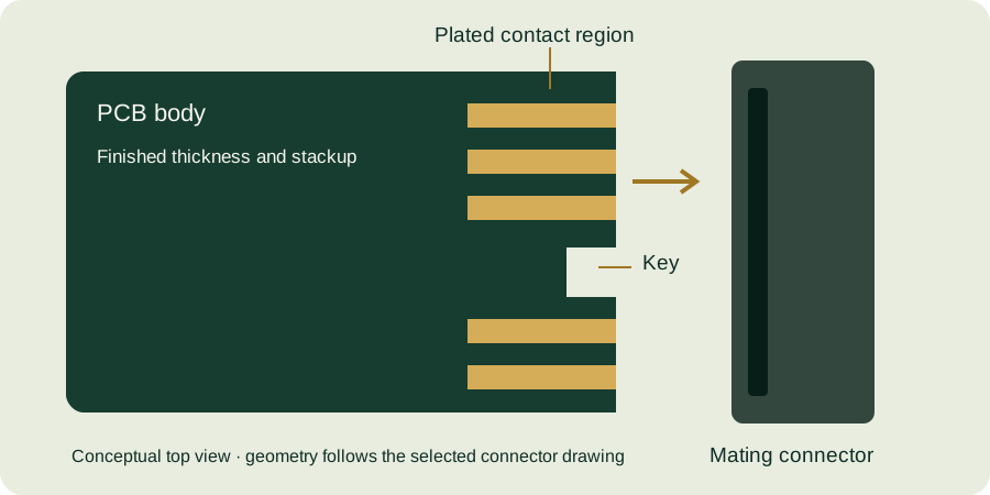
Contact geometry: pitch is not pad width
| Drawing term | Meaning | What the drawing should clarify |
|---|---|---|
| Finger or edge-contact pad | A conductive pad at the mating edge of the PCB. | The board face, contact number and portion intended to mate. |
| Pitch | Center-to-center spacing between adjacent contacts. | Whether the spacing is uniform and where numbering changes around a key. |
| Finger width | The width of an individual contact pad. | The dimension and tolerance independently of pitch. |
| Contact length | The specified extent of the contact pad along the insertion direction. | Its datum and whether the dimension includes an area affected by beveling. |
| Key notch | An interruption in the card edge used for mechanical polarization or compatibility. | Width, depth, position and corner geometry relative to defined datums. |
| Datum | A defined reference used to establish the location or orientation of a feature. | The actual reference edge, plane or centerline used by each dimension. |
Consider an illustrative design with 1.00 mm pitch and 0.70 mm finger width. For ideal, equal-width, parallel pads, the nominal edge-to-edge gap is 1.00 minus 0.70, or 0.30 mm. This arithmetic does not establish an acceptable finished gap: dimensional tolerances and the mating connector still control the design. Writing “1 mm fingers” would leave the reviewer unsure whether the author meant pitch or width.
Board thickness and bevel terminology
Finished board thickness needs a measurement convention at the connector interface. A laminate or core thickness is not automatically the finished thickness at the contact region. State the required measurement surfaces and tolerance rather than relying on a stackup label alone.
A bevel, also called a chamfer in many drawing contexts, removes material at the leading edge. The angle needs an explicit reference. A note with an angle alone may not define the remaining tip geometry. Residual tip thickness describes the material left at the leading edge after the specified bevel; the drawing should make clear whether machining is applied to one or both faces. Use the bevel geometry guide to review the relationship between the edge detail and the connector.
The distinction between the connector mounting footprint and the mating-card layout is also essential. Samtec’s HSEC1 layout document contains separate views for the connector PCB and its mating card. The mating-card view identifies a pad-to-pad thickness dimension and a bevel detail. Check the applicable connector option and drawing revision instead of transferring a dimension from an unrelated view.
Finish terms: specify the deposit and its location
Selective plating means the specified plating applies to designated regions. Identify those regions in the fabrication package. Do not assume a finish called out for the contacts applies to solder pads, or that a general surface-finish note fully defines the mating contacts.
Hard gold identifies a contact-finish requirement that needs an agreed deposit specification. ENIG names a different finish process and should not be treated as a shorthand for the same contact system. The drawing should distinguish finish requirements where both contact and solderable regions occur; see the hard gold and ENIG comparison.
Nickel underplate is the layer beneath the gold in a nickel-gold system. Samtec explains the barrier role of nickel in its connector underplating discussion. A connector manufacturer’s process recommendation is not automatically the required thickness for a PCB drawing. Specify the board’s nickel requirement separately from its gold requirement.
Minimum, nominal and measurement location
A nominal value is a stated target or reference value; a minimum is a lower acceptance limit under the agreed measurement procedure. Do not silently convert a nominal plating note into a minimum requirement. The words affect what the supplier must make and what inspection can accept.
For example, 30 microinches equals 0.762 micrometres. That conversion preserves the amount, not the acceptance meaning. “30 microinches nominal” and “0.762 micrometres minimum” are therefore not interchangeable instructions. Use the gold plating thickness guide for unit handling, and define where measurements are taken rather than relying on a single unspecified average.
Process features versus final contact features
A plating bus or tie bar is a manufacturing feature associated with providing an electrical path during electroplating. Clarify which features belong to the production panel and which must remain on the finished board. Review the removal method and final edge condition with the fabricator; a manufacturing connection should not be confused with a circuit connection in the delivered design.
A keepout also needs a defined scope. A component keepout, solder-mask clearance and copper keepout restrict different things. Identify the affected layer or material and dimension the applicable region. “Keep clear near fingers” is difficult to inspect because it does not say what is prohibited or where the boundary lies.
A practical drawing-language review
- Replace ambiguous phrases such as “standard fingers” with references to the exact connector and controlled drawing.
- Check that pitch, width, length and key position are separate requirements with a consistent viewing direction.
- Define finished thickness and the bevel detail using explicit measurement references.
- Mark selective finish boundaries; distinguish gold, nickel and the finish elsewhere on the PCB.
- Identify minimum versus nominal values, units, inspection locations and agreed acceptance evidence.
- Resolve conflicting notes across Gerbers, stackup sheets and mechanical PDFs before release.
Try the design-readiness checklist and thickness converter, then request a review of your gold finger PCB drawing. Share the unresolved requirements in the unified inquiry form; attachments are optional. For the broader interface context, return to the Gold Finger PCB engineering resources.
Continue with our gold finger PCB design guide and engineering tools.