
Contact pitch is the distance between neighboring contact centers. Finger width is the width of an individual conductive pad. Treating these as the same dimension can produce an incorrect gap, an inaccurate plating-area estimate or a footprint that does not match its connector. A fabrication drawing should identify both dimensions and their applicable tolerances.
Calculate the nominal gap correctly
For parallel rectangular contacts of equal width, the nominal edge-to-edge gap is pitch minus width. If an illustrative pattern has a 1.20 mm pitch and a 0.75 mm width, the nominal gap is 0.45 mm. This equation assumes the contact edges being compared have the same orientation and a constant width at the measurement location.
If neighboring contacts have different widths, use pitch minus half of each width: gap = p − w1/2 − w2/2. With 1.20 mm pitch and widths of 0.70 and 0.80 mm, the result is again 0.45 mm. Do not apply the rectangular-pad calculation across a key notch or to a tapered region without accounting for the actual geometry.
Nominal spacing is not the minimum finished spacing
Suppose the illustrative equal-width pattern allows pitch of 1.20 ± 0.02 mm and each contact width of 0.75 ± 0.03 mm. Under a simple independent worst-case assumption, the smallest gap is 1.18 − 0.78 = 0.40 mm. The largest is 1.22 − 0.72 = 0.50 mm. These are arithmetic bounds for the stated model, not a manufacturing recommendation.
Actual drawings may control contact centers with position tolerances rather than a separately toleranced adjacent pitch. In that case, construct the stackup from those controls; do not add a second pitch allowance for the same underlying error. State whether dimensions refer to artwork or the finished conductive feature, since production acceptance should use the agreed finished-feature definition.
Pitch does not establish the whole contact field
For one uninterrupted row of N equally spaced contacts, the center-to-center span from first to last is (N − 1) × pitch. Ten contacts on 1.20 mm pitch span 10.80 mm between the outer centers. With 0.75 mm equal-width end contacts, the outer-edge span is 11.55 mm. Confusing contact count with the number of spaces introduces a one-pitch error.
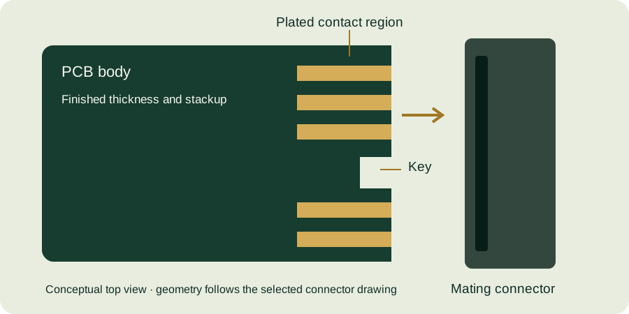
The mating-card view in Samtec’s HSEC1 layout drawing identifies contact geometry and key-related features. Use the actual drawing to locate interrupted arrays; the simple uninterrupted-row equation does not specify where a key belongs.
Carry the distinction into purchasing and inspection
| Activity | Use pitch for | Use width for |
|---|---|---|
| CAD review | Contact-center distribution | Individual pad shape |
| Inspection planning | Relative center locations | Finished contact boundaries |
| Area estimate | Locating the array only | Calculating each plated rectangle with its length |
A quote request that lists only pitch cannot define plated area. A width measurement alone cannot establish correct contact registration. Include the drawing and the connector reference rather than expecting one number to represent the entire interface.
Quick review checklist
- Label pitch and finger width independently.
- Count spaces, not contacts, when calculating a center span.
- Check the geometry on both sides of every key.
- Use a tolerance model that does not double-count errors.
- Define the finished feature and inspection location.
Review the contact geometry guide and inspection planning overview. For an ambiguous pattern, submit the dimensioned drawing for review rather than specifying “standard fingers.”
Continue with our gold finger PCB design guide and engineering tools.