
Contact length, engagement and wiping distance describe different parts of a card-edge interface. A long gold finger does not mean that the connector touches its entire length. The actual contact track depends on connector geometry, the insertion path and the final assembly position. Keeping these terms separate helps avoid incorrect finish boundaries and misleading lifetime assumptions.
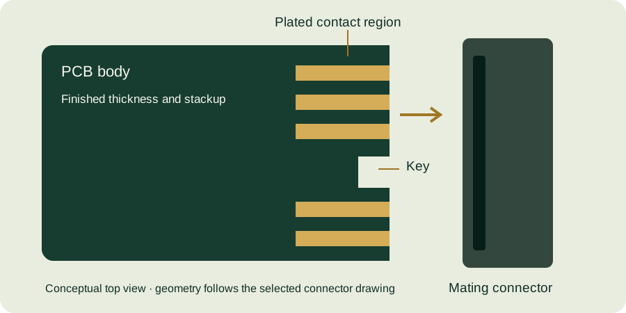
Define the three quantities
| Term | Meaning in the review | Evidence needed |
|---|---|---|
| Contact pad length | Extent of the PCB conductive feature along insertion | Controlled mating-card artwork and drawing |
| Final engagement | Relationship of the connector contact to the card at its seated position | Connector geometry and assembly position |
| Wiping distance | Relative sliding travel over the contact surface during the defined mating movement | Connector design information or suitable system evaluation |
Terminology can vary between suppliers. If a datasheet uses “engagement length,” check what that dimension actually references. Do not substitute your own definition without recording the translation in the interface review.
Use a travel diagram rather than pad length alone
For an illustrative one-dimensional model, place coordinate zero at a stated board reference. Suppose the plated region extends from x = 1.0 to 6.0 mm, initial sliding contact occurs at x = 1.8 mm and the final nominal contact position is x = 4.8 mm. The modeled travel along the pad is 3.0 mm, while the plated region is 5.0 mm long. Neither value should be renamed as the other.
If the final location can vary from 4.5 to 5.1 mm, that variation must be included when checking the finished contact zone. The model does not describe a real connector’s changing spring shape or pressure distribution. It simply shows why the plated boundary and the possible contact positions should be compared explicitly.
Include mechanical stops and tolerances
An enclosure stop, mounting screw or guide rail can affect where the card finally sits. Review the complete positional stack rather than assuming the connector alone controls insertion depth. If a drawing permits movement, consider the relevant extremes when checking whether the contact remains in the intended finished region.
Samtec’s HSEC1 document provides mating-card geometry, including a bevel detail. A mating-card layout is one input to the interface review; it should not be treated as a universal wiping-distance or service-life specification.
A wear track is evidence, with limits
After a controlled mating exercise, photographs of a visible track may help locate where interaction occurred. Record the connector, board revision, number of operations and handling conditions. A track alone does not establish acceptable contact resistance, sufficient finish thickness or remaining useful life.
Do not deliberately scratch or polish the production contact to “make the track clearer.” Keep inspection samples and test conditions controlled, and separate visual observations from electrical or mechanical acceptance criteria. See the inspection planning guide for organizing different types of evidence.
Contact-zone review checklist
- Define the pad length using an explicit board datum.
- Identify initial and final contact positions from appropriate connector information.
- Include assembly constraints and tolerances.
- Keep the relevant contact travel within the approved finish region.
- Document tests without converting wear appearance into an unsupported lifetime claim.
Continue with the card-edge design guide and finish specification guide. Request a review of the contact region with the connector reference and assembly constraints included.
Continue with our gold finger PCB design guide and engineering tools.