
A gold finger contact pattern is a mating interface, not a collection of pads that can be freely resized. Its location and geometry must agree with the connector’s contacts and housing. Changing a pad to simplify routing or reduce plated area can create a mismatch even when the PCB still meets general manufacturing rules.
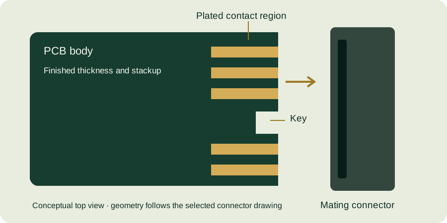
List the coupled dimensions
Contact pitch establishes an array relationship, but pitch alone is not the interface. Finger width, length, edge position, card thickness, key features and bevel geometry can all affect mating. Treat these as a coordinated set of requirements. A change to one field should prompt a check of the others that depend on it.
The appropriate starting point is the selected connector’s mating-card information. For example, Samtec publishes a MEC1 layout document for a defined family and configuration. Verify the exact ordering option and revision; the existence of a family drawing does not establish interchangeability with another connector.
Example: a narrow-pad proposal
Imagine a design team proposes reducing an illustrative finger width from 0.80 to 0.60 mm while retaining the same center positions. The nominal plated rectangular area falls by 25 percent if length and count remain constant. That arithmetic explains an area change, but it does not establish that the narrower pad is acceptable.
The review must ask whether the connector’s contact footprint and its permitted position variation remain compatible with the new conductive region. It must also check whether the proposed dimensions comply with the controlled mating-card requirements. If the drawing specifies the original width, changing it requires a documented design decision rather than an informal manufacturing optimization.
Actual cost savings cannot be inferred from the percentage area change alone. Setup, processing, inspection and other board costs remain part of the quotation. Use the theoretical gold mass tool only for its stated arithmetic purpose.
Do not use spring compliance as an unspecified allowance
Connector contacts are designed to move under defined conditions. That does not grant unlimited tolerance for PCB thickness or positional error. Use published requirements or obtain clarification from the connector supplier when an intended condition falls outside the documentation.
A hand-assembled prototype that seems to fit is a useful observation, not proof that all allowed production extremes will work. Record which parts and dimensions were tested, then compare them with the full permitted ranges. Avoid forcing a board into a connector to demonstrate compatibility.
Keep routing changes behind a controlled boundary
Where possible, treat the approved mating region as a controlled CAD block. Route into it using the available design space while preserving the specified contact geometry. If electrical or mechanical constraints make that impossible, raise the issue before release rather than altering a pad silently.
After any approved change, review the manufacturing export as well as the CAD library. An updated footprint in the library does not prove an already released board file has changed. Record the board revision and check that the fabrication package contains the intended version.
Geometry-change checklist
- Identify the controlled dimensions affected by the proposal.
- Compare the change with the exact connector documentation.
- Check permitted positional and thickness extremes.
- Separate area arithmetic from cost and performance claims.
- Obtain and retain the required technical approval.
- Verify the released artwork and drawing together.
Continue with the gold finger design guide and manufacturing review overview. Submit a proposed geometry change with the current and revised dimensions clearly identified.
Continue with our gold finger PCB design guide and engineering tools.