
A PCB manufacturer’s general design rules describe what a manufacturing process can produce. A connector drawing describes the interface a particular connector expects. A gold finger PCB must satisfy both. A manufacturable pad pattern can still be the wrong mating pattern, and a correct connector interface may still need a process discussion before the board can be built.
The useful question is therefore not which document is universally more important. It is which document controls each requirement, and whether all controlled requirements can be met together. This article gives a practical way to make that decision before releasing artwork.
Separate interface requirements from process limits
| Question | Starting document | Required follow-up |
|---|---|---|
| Where should each finger sit? | Applicable mating-card drawing | Confirm connector option, viewing direction and datums. |
| Can the supplier hold the finished geometry? | Supplier capability review | Obtain agreement for the actual stackup, outline and quantity. |
| What board thickness enters the connector? | Connector interface specification | Define measurement surfaces and tolerance in the fabrication package. |
| How is selective plating made? | Fabricator’s process proposal | Review temporary connections and the final delivered edge. |
| What proves the assembly works? | Product qualification plan | Test the actual board, connector and mechanical assembly. |
General minimum spacing should not be used to redesign a connector footprint without checking the mating requirements. Similarly, a downloadable CAD footprint should not be treated as evidence that every fabricator can meet its finished dimensions.
Check which board a drawing depicts
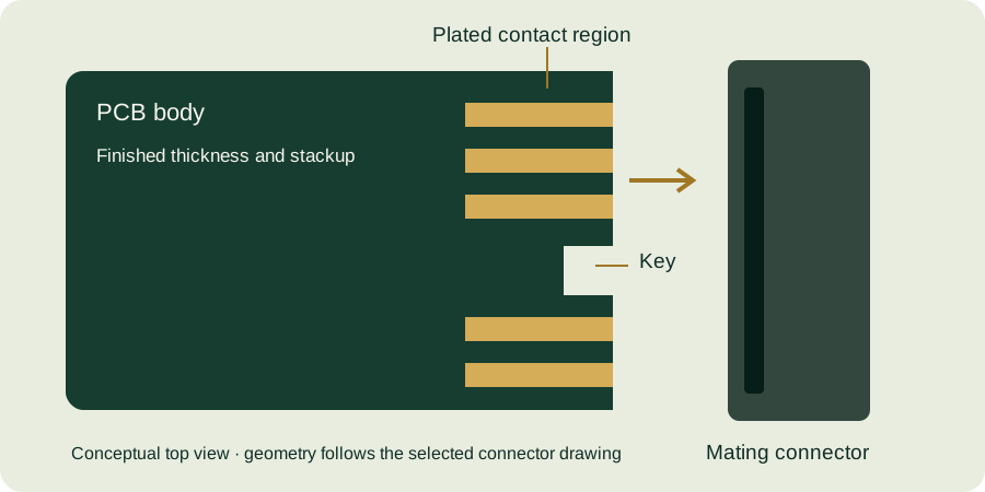
Card-edge systems involve at least two relevant PCB regions: the board carrying the connector and the card inserted into it. The mounting pads on the first board are not the fingers on the second. Samtec’s HSEC1 layout document illustrates this distinction by providing separate mounting, stencil and mating-card information. Select the view and option that match the assembly being designed.
Record the document title, revision and exact connector ordering code beside the CAD library reference. A footprint named only “edge connector” makes later checking difficult. If a drawing contains several position counts or mounting options, mark the applicable figure in the review record rather than leaving production staff to infer it.
A worked conflict-resolution example
Suppose an imaginary connector requires a finished card thickness between 1.45 and 1.65 mm. The initial fabrication proposal is 1.60 mm with a tolerance of plus or minus 0.15 mm. Its possible range is 1.45 to 1.75 mm. The ranges overlap, but the proposed board range is not entirely contained in the connector range. A nominal 1.60 mm value alone does not resolve the conflict.
The next step is to ask whether an agreed finished range can be produced and measured at the contact region. A hypothetical 1.55 mm plus or minus 0.08 mm proposal would span 1.47 to 1.63 mm and fit inside the stated interval mathematically. That is a candidate for review, not a claim that the supplier can make it or that the complete assembly is qualified. Copper, finish, local geometry and the measurement convention still matter.
Keep exceptions visible
Do not fix a conflict by silently changing the CAD footprint or deleting a drawing tolerance. Create an engineering question with the conflicting requirements, the proposed resolution and the person responsible for approval. If the connector manufacturer approves a deviation, retain that evidence with the product documentation. If no acceptable solution exists, revisit the connector or board construction before committing to production.
Release checklist
- Match the mating-card drawing to the exact connector option.
- Distinguish mounting-board pads from card-edge contacts.
- Compare full tolerance ranges rather than nominal values alone.
- Obtain a manufacturability response for unresolved interface dimensions.
- Carry approved deviations into all affected release files.
- Define the assembly checks required before production approval.
Continue with the gold finger PCB design guide, bevel review and selective plating process overview. For a drawing conflict, submit the relevant files through the unified inquiry form and identify the unresolved requirement.
Continue with our gold finger PCB design guide and engineering tools.