
“1.6 mm PCB” is a common shorthand, but it is not a complete card-edge thickness requirement. The connector interacts with the finished mating region, while a stackup document may list laminate, copper or total board values under different conventions. A clear gold finger PCB drawing says what is being measured, where it is measured and which limits apply.
Identify the measurement surfaces
Start with the connector manufacturer’s definition. Does its mating-card requirement refer to pad-to-pad thickness, an unplated board section or another named surface? Samtec’s HSEC1 mating-card drawing explicitly labels a pad-to-pad thickness. This is a product-specific convention, not a universal rule for every connector.
Transfer the applicable convention into the fabrication package. A note such as “finished thickness measured between opposing contact surfaces in the defined inspection zone” is more useful than an unexplained nominal board value, provided that it matches the selected connector and the agreed inspection method.
Do not add layers twice
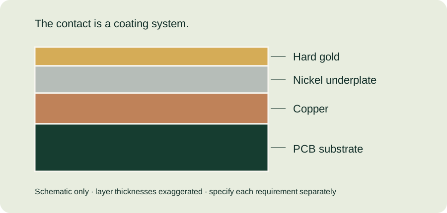
An illustrative stack calculation begins with 1.50 mm between two stated substrate reference surfaces. Suppose the specified conductive build above each reference surface is 0.035 mm. The arithmetic distance between the resulting outer surfaces is 1.50 + 0.035 + 0.035 = 1.57 mm. This simplified model is only valid if the starting thickness excludes those outer builds.
If the supplier’s starting value already includes finished copper, adding copper again overstates the result. If a stackup value excludes a separately applied contact finish, that finish needs appropriate treatment. Ask what each number includes rather than applying a universal stackup formula to differently defined inputs.
Location matters as much as arithmetic
A thickness measurement on a masked region away from the fingers can answer a different question from a measurement across contact pads. A reading at a bevel tip describes a different geometry again. Mark a suitable contact-region measurement location and avoid damaged, tapered or otherwise unrepresentative surfaces unless those features are specifically being inspected.
Also distinguish thickness from flatness, bow or twist. A single thickness value does not establish whether the whole card enters the connector without interference. Keep the bevel detail and the assembly alignment checks in the mechanical review.
Define the tolerance and its evidence
| Drawing item | Question to settle |
|---|---|
| Finished thickness | Which two surfaces define the measurement? |
| Acceptance limits | Are both lower and upper limits explicit? |
| Location | Which contact-region positions are inspected? |
| Method | What instrument and setup are appropriate to the feature? |
| Reporting | Are individual readings or a summary required? |
An instrument display with extra decimal places does not establish measurement capability. The supplier should use a suitable, controlled method and agree how uncertainty is handled when readings approach a limit. Do not turn a nominal stackup estimate into an inspection result.
Thickness-note checklist
- Confirm the exact connector and mating-card specification.
- Identify included copper and finish layers in the stackup values.
- Define measurement surfaces and contact-region locations.
- Specify the agreed finished limits.
- Review bevel, alignment and assembly fit separately.
Use the multilayer stackup guide and inspection overview to prepare your requirements. Submit the stackup and connector drawing for a thickness review through the unified inquiry form.
Continue with our gold finger PCB design guide and engineering tools.