
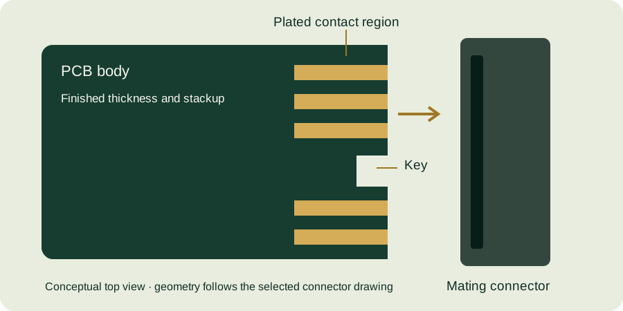
Gold fingers and plated PCB edges are different manufacturing features. Gold fingers are defined contact areas on the board faces near a mating edge. Edge plating places conductive material on specified board sidewalls. Both involve metal near the perimeter, but they require different geometry, process planning and acceptance information.
Distinguish the surface being specified
| Feature | Surface to identify | Main drawing question |
|---|---|---|
| Gold finger contacts | Defined contact regions on one or both external faces | Which connector geometry and contact finish apply? |
| Plated board edge | Defined vertical or profiled sidewall sections | Which perimeter segments are metallized and electrically connected? |
| Ordinary routed edge | Finished laminate outline without specified sidewall metallization | What copper clearance and edge condition are required? |
Do not use the phrase “gold edge” as the only fabrication instruction. It could be read as a contact finish, a sidewall finish or an appearance request. Mark the intended surfaces in a drawing and keep the finish specification separate from the geometric definition.
Process planning differs
Eurocircuits describes round-edge plating as metallization of the PCB contour, with routing carried out before the relevant metallization stage. Its separate edge-connector gold plating guide describes selective contact plating. These are supplier process descriptions, not a declaration of this site’s manufacturing capability or universal limits.
For an actual order, ask the fabricator to review the requested combination. Panel support, profiling sequence, selective finish access and the final edge condition may all need agreement. Do not assume that adding a gold-finger note automatically orders sidewall plating.
A drawing example with two distinct requirements
Consider a hypothetical module with card-edge contacts along its lower edge and a separate conductive sidewall region along part of its left edge. Label the lower face-contact area as region A and the specified sidewall segment as region B. The drawing should define the limits of both regions, their required finishes and any intended electrical connections.
If region B is intended to connect to ground, identify the actual copper network and required connectivity. Merely coloring an outline in a mechanical PDF does not create that connection in the PCB data. Check that unrelated internal conductors remain isolated from the metallized region under the agreed design and manufacturing rules.
If a beveled contact edge intersects a plated sidewall region, explicitly review the transition. Do not leave the supplier to infer whether plating should remain, terminate or be removed by the later operation. The released package must describe the final delivered part.
Inspection must match the feature
For the fingers, inspect the agreed contact geometry and finish evidence. For a plated sidewall, define coverage, connectivity and other acceptance requirements appropriate to that feature. A photograph of gold-colored face pads cannot demonstrate sidewall metallization, and electrical continuity alone cannot establish the full finish specification.
Keep the inspection plan tied to labeled drawing regions. This makes a nonconformance report more useful: “region B interrupted at the stated location” is clearer than “edge plating bad.” Include reference photographs and measurements without assuming the failure mechanism from appearance alone.
Specification checklist
- Identify face contacts and sidewall regions separately.
- Dimension the start and end of every special finish region.
- Define required electrical connections and exclusions.
- Review panel, profiling and bevel interactions with the fabricator.
- Agree inspection evidence for each feature type.
See the gold finger PCB overview, bevel guide and manufacturing process overview. Submit a marked-up fabrication drawing through the unified inquiry form to clarify the requested edge features.
Continue with our gold finger PCB design guide and engineering tools.