
Single-sided and double-sided edge contacts describe the faces of the PCB carrying contact pads. They do not describe the board’s total copper layer count, and they do not by themselves establish the connector’s contact arrangement. A multilayer board can have contacts on one face, while a board with pads on both faces may connect those pads to different signals or to the same net.
Choose the arrangement from the required connector interface and circuit mapping. Do not remove a row of fingers to save plating area until the connector, mechanical and electrical implications have been reviewed.
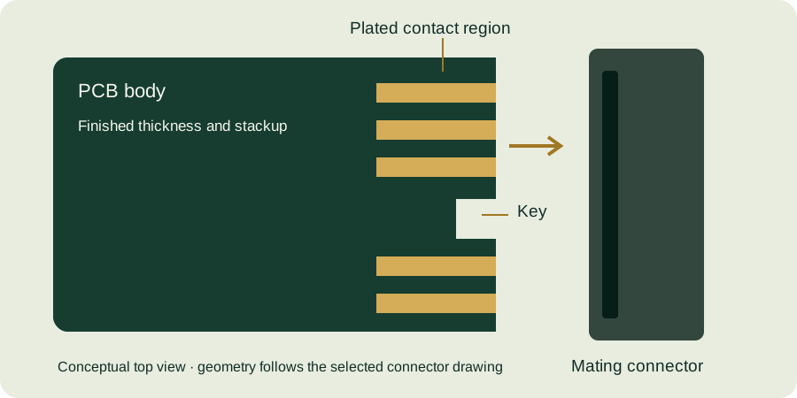
Three different counts to keep separate
| Count | What it describes | Why it matters |
|---|---|---|
| PCB copper layers | The conductive layers in the stackup | Routing, planes and finished construction |
| Contact-bearing faces | The external faces with mating pads | Artwork and selective finish regions |
| Electrical contact positions | The contacts assigned in the interface pin map | Signal mapping and connector selection |
A drawing note saying “20 gold fingers” is ambiguous if it does not state whether that means twenty total or twenty per face. Specify the count for each face and identify positions around any key notch. Keep the numbering convention consistent between schematic, PCB layout and test documentation.
Opposing pads need independent verification
Two pads directly opposite each other through the board thickness are not automatically connected. If the design connects them, the connection must exist in the copper artwork and netlist. If they carry different nets, the fabrication drawing must not encourage a reviewer to treat them as a single position.
The HSEC1 mating-card drawing shows numbering for the two card faces. It is an example of why viewing direction and numbering must be checked in the applicable product document rather than inferred from a generic illustration.
An area calculation that exposes a common quoting error
Imagine a board with twelve rectangular plated contacts on its top face and twelve on its bottom face. If each specified plated rectangle is 0.80 mm wide and 4.00 mm long, the ideal total rectangular area is 24 × 0.80 × 4.00 = 76.8 mm². Counting only one face gives 38.4 mm², half the intended area.
This example is arithmetic, not a recommended contact size or a complete plating-cost model. Actual plated boundaries may extend beyond the functional contact rectangle, and a quote may include process features, setup, inspection and other operations. The gold mass estimator needs an area consistent with the intended finish region; it cannot determine the connector geometry for you.
Thickness and finish still belong to the whole interface
For contacts on opposing faces, identify where the finished thickness is measured. A bare laminate thickness does not necessarily represent the distance between the two finished mating surfaces. Coordinate the stackup and surface-finish notes with the connector specification rather than assuming a nominal board thickness is sufficient.
If the two faces have different selective finish boundaries, show both explicitly. Do not rely on a note saying “bottom same as top” when the artwork is intentionally asymmetric. The same caution applies to contact lengths and keying features.
Review before release
- State contact count per face and total count.
- Label top and bottom views, including viewing direction.
- Check opposing-pad net assignments against the schematic.
- Confirm the selected connector supports the intended contact arrangement.
- Include both faces in finish-area estimates.
- Define finished thickness and selective plating boundaries.
See the multilayer board planning guide for stackup context and the plating thickness guide for finish terminology. Send both contact-face views for a fabrication review through the unified inquiry form.
Continue with our gold finger PCB design guide and engineering tools.